Background
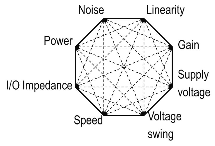
With its stringent requirements on the energy consumption of electronic devices, the Internet of Things (IoT) has become the primary driver for the design of low-power analog and RF circuits, making the analog/RF design exercise ever more challenging. In fact, an optimum design targets the best trade-off between several aspects, usually represented by gain, current efficiency, bandwidth, linearity and noise performance. To achieve this, designers often start using simple transistor models before fine-tuning with the design-kit.

However, due to the down-scaling of CMOS processes and the reduction of the supply voltage, the operating point has progressively pushed from the traditional strong inversion region towards moderate and even weak inversion, where the simple quadratic model is obviously no more valid.
Objective
The objective of the low-power and low-voltage analog/RF IC design activity is to minimize the power consumption of analog circuits and systems implemented in deep submicron CMOS technologies. It also explores techniques that can make circuits operate at very low-voltage without penalty on the power consumption.
Directions of Research
- Building a simplified EKV Model for early-stage design phase
- Design of Analog/RF circuits targeting low-power and low-noise operation